The global artificial intelligence boom is creating a new battle in the semiconductor industry. While much of the attention has focused on powerful AI processors, graphics processing units (GPUs), and advanced manufacturing technologies, another part of the chip supply chain is becoming equally important: advanced semiconductor packaging.
As demand for AI computing continues to grow, chipmakers are facing a critical challenge. Producing powerful processors is no longer enough. Companies must also connect processors, memory, and other components inside increasingly complex packages that can transfer enormous amounts of data efficiently.
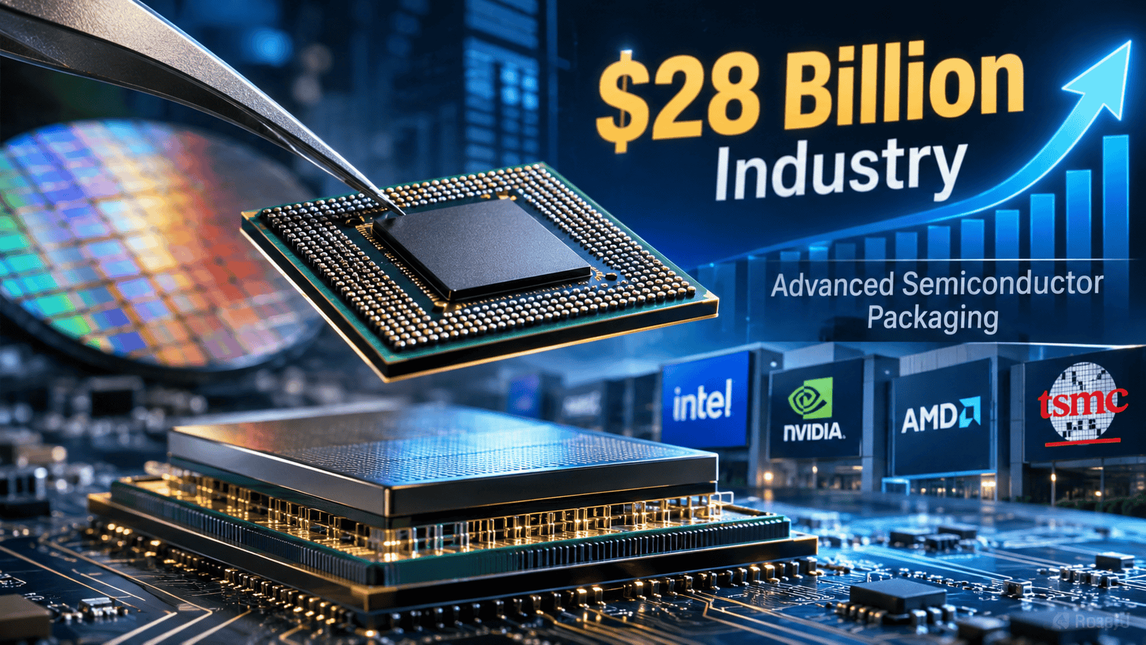
Industry investment in advanced packaging is expected to approach $28 billion in 2026, reflecting the growing importance of this technology. Revenue from advanced packaging is also forecast to exceed traditional semiconductor packaging revenue for the first time this year.
This shift could reshape the semiconductor supply chain, create new investment opportunities, and intensify competition among leading technology companies.
Why Advanced Semiconductor Packaging Matters for AI
For decades, semiconductor packaging primarily protected chips and provided the electrical connections needed to attach them to circuit boards. However, the growing complexity of artificial intelligence systems has transformed its role.
Modern AI processors require enormous computing power and rapid access to high-bandwidth memory. Connecting multiple processors and memory components within a single package helps reduce communication delays and improve overall performance.
Advanced packaging makes this possible by combining several silicon components into one integrated system. Instead of relying entirely on a single large chip, manufacturers can connect multiple chiplets and memory stacks to deliver greater computing capabilities.
This approach is particularly important for AI data centers, where processors must handle demanding workloads such as training large language models, generating AI responses, processing images, and running autonomous systems.
As chip designs become more sophisticated, packaging technology is emerging as a major factor in determining performance, production costs, and manufacturing capacity.
The $28 Billion Investment Opportunity
The growing importance of advanced packaging is attracting significant investment from semiconductor manufacturers and equipment suppliers.
Industry forecasts indicate that capital spending on advanced packaging technology could approach $28 billion in 2026. This investment reflects increasing demand for more sophisticated AI processors and the need to expand production capacity.
The opportunity extends beyond traditional chip manufacturers. Companies producing semiconductor equipment, materials, testing systems, and packaging technologies could also benefit from the industry’s expansion.
For investors, this creates a broader semiconductor investment landscape. The AI boom is no longer limited to companies designing processors or manufacturing chips. Businesses operating in the packaging and equipment segments may become increasingly important to the next stage of AI infrastructure development.
However, higher investment does not automatically guarantee strong returns. Manufacturers must manage production costs, technological challenges, customer demand, and the risk of excess capacity.
TSMC’s CoWoS Technology Takes Center Stage
Taiwan Semiconductor Manufacturing Company (TSMC) remains a major player in advanced semiconductor packaging through its Chip-on-Wafer-on-Substrate (CoWoS) technology.
CoWoS allows manufacturers to integrate processors and high-bandwidth memory within a sophisticated package. This enables faster communication between components and supports the performance requirements of modern AI accelerators.
The technology is widely used across the AI semiconductor ecosystem, including products associated with NVIDIA, AMD, and Broadcom.
TSMC’s position gives it considerable influence over the supply chain. However, the rapid expansion of AI computing demand is putting pressure on available advanced packaging capacity.
This has encouraged chip designers to explore additional suppliers and alternative manufacturing approaches.
The situation highlights an important development in the AI industry: packaging capacity can become a production bottleneck even when demand for processors remains strong.
NVIDIA Looks Beyond Traditional Supply Channels
NVIDIA’s growing demand for advanced packaging illustrates how important this part of the supply chain has become.
According to a Reuters report published on November 6, NVIDIA is providing billions of dollars in financing to support the expansion of CoWoS packaging capacity at Siliconware Precision Industries (SPIL), a subsidiary of Taiwan’s ASE Technology.
The reported financing is intended to support additional factory space and equipment. NVIDIA and ASE had not publicly confirmed the reported arrangement at the time of the report.
If expanded capacity becomes available, it could help address a critical constraint affecting the production of advanced AI processors.
The development also demonstrates how major chip designers may become more directly involved in financing and expanding the manufacturing infrastructure required by their products.
For the broader industry, this could encourage closer partnerships between chip designers, packaging companies, and equipment manufacturers.
Powertech and Broadcom Explore New Packaging Technology
Competition is also creating opportunities for smaller semiconductor suppliers.
Taiwan-based Powertech Technology is developing panel-level packaging, an approach that uses larger rectangular panels rather than traditional round silicon wafers.
The technology could allow manufacturers to process more chips in each production run while reducing material waste. These advantages may become increasingly important as AI processors grow larger and more complex.
Powertech is working with AMD and Broadcom on advanced packaging development. The company also plans a $400 million joint venture with Broadcom in Singapore, with production targeted for 2028.
Meanwhile, TSMC is developing its own panel-based packaging technology, known as Chip-on-Panel-on-Substrate (CoPoS).
Although these technologies still face manufacturing and scaling challenges, they illustrate how the semiconductor industry is searching for alternatives that can support future AI hardware requirements.
What This Means for Semiconductor Investors
The expansion of advanced packaging could create opportunities across several segments of the technology industry.
1. Semiconductor packaging companies
Companies providing advanced packaging services may benefit from increased demand as chip designers seek additional production capacity. Suppliers with established manufacturing capabilities and strong relationships with major customers could gain a competitive advantage.
2. Semiconductor equipment manufacturers
Advanced packaging requires specialized equipment for bonding, inspection, testing, and material processing. Equipment suppliers could benefit as manufacturers invest in new facilities and production lines.
3. AI chip designers
NVIDIA, AMD, and Broadcom depend on sophisticated packaging technologies to deliver increasingly powerful processors. Greater packaging capacity could support product shipments and help reduce supply constraints.
4. Semiconductor materials suppliers
The growing complexity of chip packages is increasing the importance of advanced substrates, interconnect materials, and other specialized components. Suppliers operating in these areas may find new growth opportunities.
Investors should nevertheless evaluate company valuations, capital requirements, customer concentration, and manufacturing execution before making investment decisions.
Key Risks: High Investment Does Not Guarantee High Returns
Despite the industry’s growth potential, advanced packaging is not without risks.
Building new facilities requires substantial capital investment, and manufacturing processes must achieve reliable yields before production can scale commercially.
There is also a risk that companies could expand capacity faster than long-term demand develops. If AI infrastructure spending slows, some manufacturers may face underutilized facilities and pressure on profitability.
Technological competition presents another challenge. Companies are developing different packaging approaches, and today’s leading technology may face stronger competition as alternatives mature.
Geopolitical tensions and the concentration of semiconductor manufacturing in Asia also remain important considerations for global investors.
The companies most likely to benefit will be those that combine technological expertise with disciplined investment, reliable production, and strong customer relationships.
The Future of AI Infrastructure Depends on More Than Powerful Chips
The semiconductor industry is entering a new phase in which packaging technology is becoming a strategic component of AI development.
As artificial intelligence models become larger and data centers demand greater computing capacity, manufacturers will need more efficient ways to connect processors, memory, and other components.
TSMC’s CoWoS technology, NVIDIA’s reported support for additional packaging capacity, and Powertech’s panel-level packaging development demonstrate how competition is expanding beyond traditional chip manufacturing.
The expected $28 billion investment in advanced packaging during 2026 signals that companies are preparing for a more complex semiconductor market.
For global investors, the central opportunity may lie not only in identifying the next leading AI chip designer, but also in recognizing the suppliers and technology companies that make advanced AI hardware possible.
The next AI chip war may therefore be fought not just over who designs the fastest processor, but over who can package, connect, and manufacture these increasingly powerful systems at scale.
Frequently Asked Questions (FAQs)
1. What is advanced semiconductor packaging?
Advanced semiconductor packaging is a manufacturing process that connects multiple chips, processors, memory components, or chiplets within a single package to improve performance, data transfer, and integration.
2. Why is advanced packaging important for AI chips?
AI processors require fast communication between computing components and high-bandwidth memory. Advanced packaging helps reduce data-transfer bottlenecks and supports the performance demands of modern AI systems.
3. Why is the advanced packaging industry attracting investment in 2026?
Growing demand for AI processors is increasing the need for packaging capacity. Industry capital spending on advanced packaging is expected to approach $28 billion in 2026.
4. What is TSMC’s CoWoS technology?
CoWoS, or Chip-on-Wafer-on-Substrate, is TSMC’s advanced packaging technology that integrates processors and high-bandwidth memory within a single package for high-performance computing and AI applications.
5. Which companies could benefit from advanced semiconductor packaging?
Potential beneficiaries include TSMC, ASE Technology, Powertech Technology, NVIDIA, AMD, Broadcom, and semiconductor equipment manufacturers. Their individual prospects depend on production capacity, customer demand, technology development, and financial performance.
6. Is advanced semiconductor packaging a long-term investment opportunity?
It could become an important long-term growth area as AI computing expands. However, investors should consider valuation, capital expenditure, competition, production risks, and the possibility of slower AI infrastructure spending before making investment decisions.
Author: Anam Younas
Anam Younas covers business, finance, technology, and global market developments for Daily Press.
Follow Daily Press on X for the latest news and updates: @dailypressit.